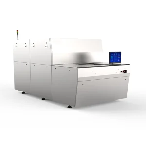
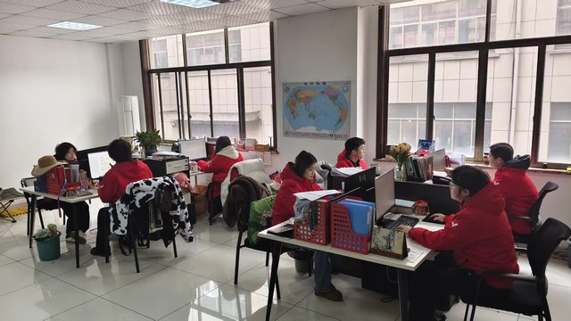
Hangzhou Focus Laser Co., Ltd. is a professional manufacturer specializing in advanced laser processing equipment for the electronics and display industries. The company focuses on the development and production of PCB laser cutting machines and glass laser cutting systems, delivering high-precision solutions for micro-electronics manufacturing and optical material processing.
In the rapidly evolving landscape of Semiconductor Packaging Laser Cutting Solutions, precision is not just a requirement—it is the baseline for survival. As global demand for smaller, more powerful electronic devices grows, the role of laser technology in semiconductor backend processing has become pivotal. We bridge the gap between complex engineering requirements and mass-market scalability.
Processing Accuracy
Heat Affected Zone
Industrial Production
Global Export Regions
The global semiconductor packaging market is currently undergoing a massive transformation. With the rise of AI-driven computing, 5G telecommunications, and the Internet of Things (IoT), traditional mechanical dicing methods are being phased out in favor of laser-based solutions. Semiconductor Packaging Laser Cutting Solutions are now the industry standard for handling fragile materials like wafer-level packages, SiP (System-in-Package), and high-density IC substrates.
From Silicon Valley to the tech hubs of East Asia, factories and exporters are seeking equipment that minimizes thermal damage while maximizing throughput. Laser cutting provides a "non-contact" advantage, which is essential when dealing with the extreme miniaturization of components where physical stress can lead to micro-cracks or delamination.
Supporting the latest WLCSP technologies with zero-edge chipping and high-speed throughput for 8-inch and 12-inch wafers.
Optimized for flexible circuit processing in smartphones and wearable tech, ensuring clean cuts without carbonization.
Precise separation of multi-chip modules used in advanced RF front-ends and complex AI accelerators.
As a leading exporter, we monitor the trends that dictate global procurement needs. The following shifts are defining the future of Semiconductor Packaging Laser Cutting Solutions:
China has emerged as the world's largest hub for electronics manufacturing and a dominant force in laser technology R&D. Hangzhou Focus Laser Co., Ltd. embodies the strengths of this ecosystem:
Located in the heart of China's tech corridor, we have immediate access to high-quality optical components and electronic subsystems, allowing for faster lead times than European competitors.
Our strong R&D capabilities allow us to provide OEM and ODM services. Whether it's specialized PCB laser cutting or unique glass laser systems, we tailor the hardware and software to your specific production line.
We provide industrial-grade precision and reliability at a price point that enables global manufacturers to scale their operations without prohibitive capital expenditure.
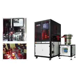
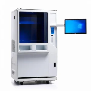
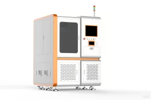
Our technologies are widely applied in PCB depaneling, flexible circuit board processing, semiconductor packaging, and precision glass cutting for smartphones, display panels, and optical components. By integrating fiber laser technology, ultra-fine beam control, and intelligent CNC systems, we ensure high cutting accuracy, smooth edges, and minimal thermal damage during processing.
Semiconductor Packaging Laser Cutting Solutions are not one-size-fits-all. Different regions and industries require specific localized approaches:
In regions like Germany and Japan, our lasers are used to cut ceramic substrates for power modules in Electric Vehicles (EVs), where high reliability under heat is critical.
For Southeast Asian assembly plants, our machines provide high-speed dicing for camera CMOS sensors and fingerprint recognition modules.
Precision cutting of medical-grade sensors and surgical tool components where bio-compatibility and burr-free edges are paramount.
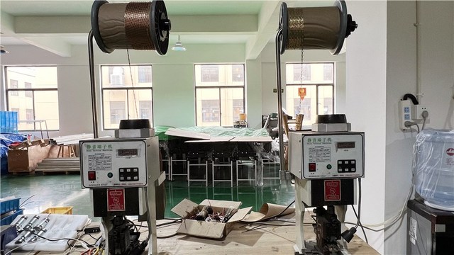
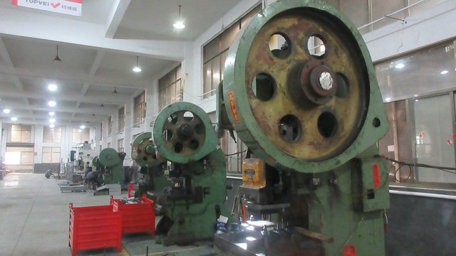
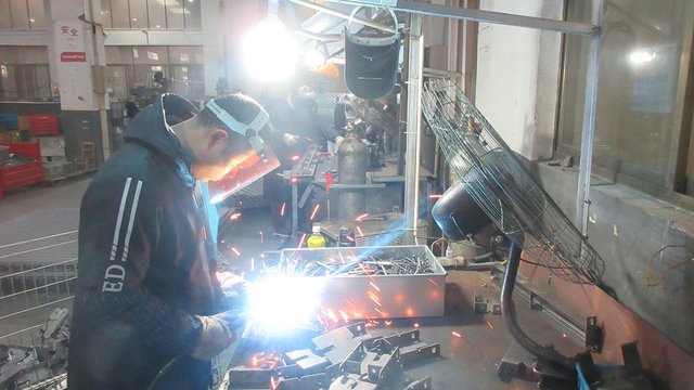
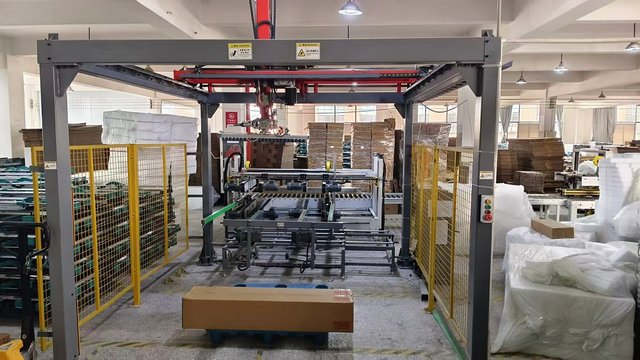
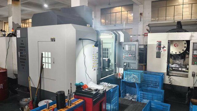
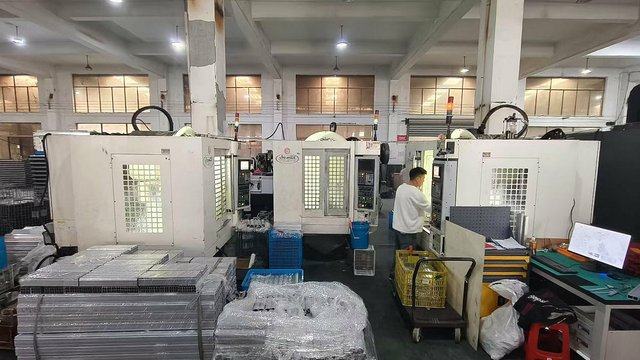
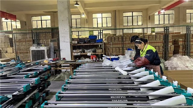
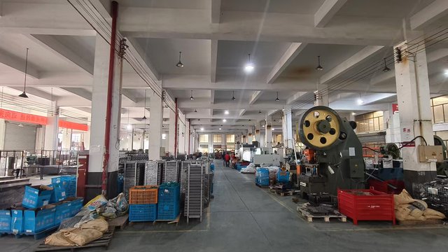
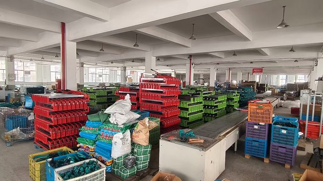
The company’s equipment is extensively used in industries such as consumer electronics, semiconductor manufacturing, automotive electronics, and smart display production. It supports both high-volume industrial production and customized precision machining requirements. Hangzhou Focus Laser Co., Ltd. emphasizes innovation, reliability, and engineering excellence. With strong R&D capabilities and strict quality control standards, we continue to advance laser micro-processing technology, aiming to become a leading global supplier of precision laser solutions.