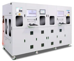
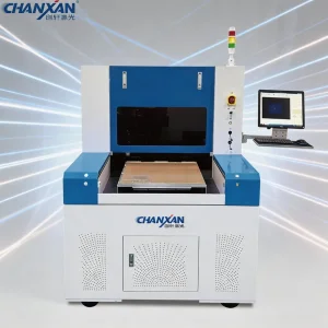
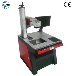
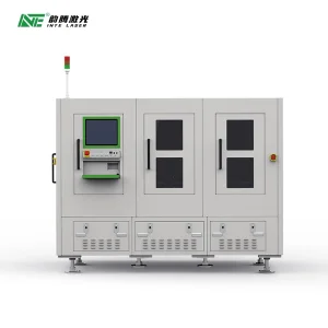
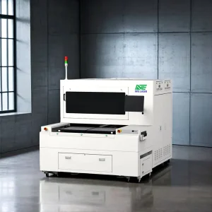
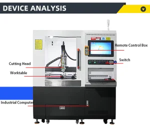
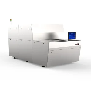
Explore our primary array of high-precision material processing machines, engineered for sub-micron accuracy, low thermal distortion, and extreme repeatability.
The industrial manufacturing sector is experiencing an unprecedented transition. As components shrink in scale and expand in material complexity, traditional mechanical cutting, milling, and etching processes have hit their physical limits. Today's global supply chains demand technologies that achieve high processing speeds without inducing thermal mechanical stress, tool wear, or structural micro-fractures in substrates. This is where ultrafast industrial laser solutions take center stage.
Hangzhou Focus Laser Co., Ltd. is a professional manufacturer specializing in advanced laser processing equipment for the electronics and display industries. The company focuses on the development and production of PCB laser cutting machines and glass laser cutting systems, delivering high-precision solutions for micro-electronics manufacturing and optical material processing.
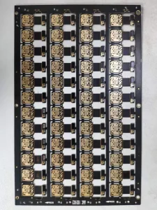
Its technologies are widely applied in PCB depaneling, flexible circuit board processing, semiconductor packaging, and precision glass cutting for smartphones, display panels, and optical components. By integrating fiber laser technology, ultra-fine beam control, and intelligent CNC systems, Hangzhou Focus Laser ensures high cutting accuracy, smooth edges, and minimal thermal damage during processing.
The company’s equipment is extensively used in industries such as consumer electronics, semiconductor manufacturing, automotive electronics, and smart display production. It supports both high-volume industrial production and customized precision machining requirements.
"By emphasizing innovation, reliability, and engineering excellence with robust R&D capabilities, Hangzhou Focus Laser Co., Ltd. provides comprehensive OEM and ODM services to meet global customer needs."
Achieving micron-level dimensional tolerances under rigorous multi-shift operations, utilizing custom-designed optical paths and stable granite stages.
State-of-the-art galvanometer scanners and high-speed CNC controls yield unmatched throughput metrics, reducing unit processing costs.
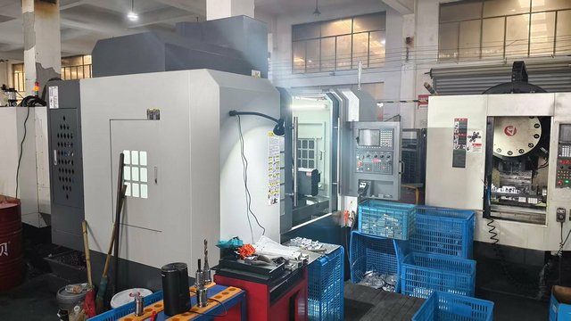
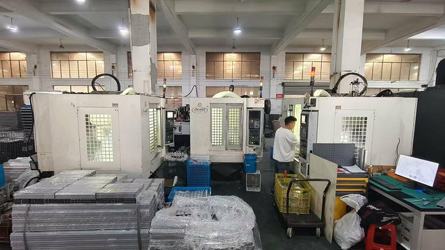
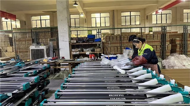
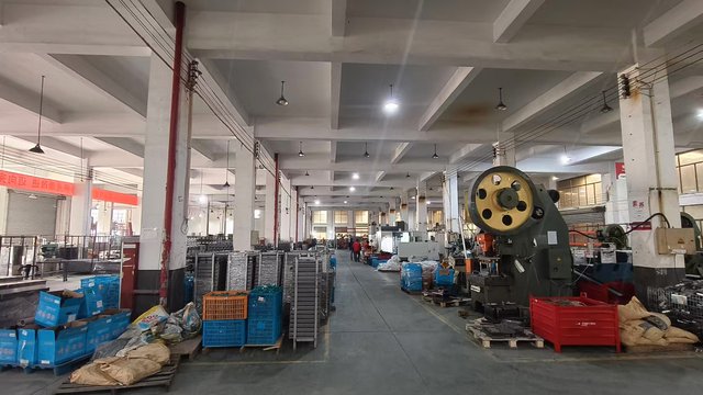
The convergence of physical manufacturing and digital logistics inside China has established a premier center for advanced industrial systems. Hangzhou Focus Laser Co., Ltd. capitalizes on this industrial matrix, optimizing component sourcing, system assembly, and rigorous testing protocols within a localized, highly integrated footprint.
Direct integration with premium component ecosystems—ranging from high-stability optical elements to precise linear stages. This localized manufacturing network shortens custom OEM design-to-build lead times significantly.
Every laser source and mechanical stage undergoes continuous burn-in testing, beam quality inspection using high-resolution beam profilers, and multi-axis alignment verification before shipment.
Engineered to adapt. Whether modifying machine frames for conveyor systems, optimizing software API connections, or engineering custom fixtures, the local team executes adaptations with high speed and cost efficiency.
For global procurement agents, this localized ecosystem means faster iterations, reduced capital expenditure (CapEx), and reliable system stability, allowing manufacturing plants to meet strict target deadlines.
Modern procurement specialists analyze total cost of ownership (TCO), machine uptime, and availability of wear parts. The global market requires flexible systems that adapt to various industrial applications, including:
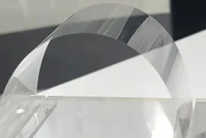
Flexible displays, OLED panel cutting, and FPCB depaneling require a process that prevents delamination and discoloration. The use of UV Picosecond Lasers solves this by using cold ablation to cleanly cut multilayer structures containing polyimide, copper, and optical adhesives.
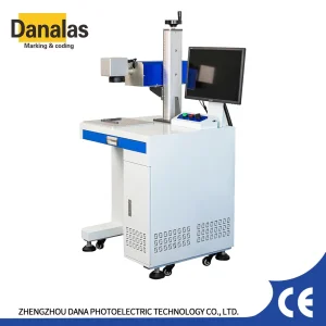
Modern vehicles contain complex sensor arrays, ADAS modules, and high-frequency communication circuits. High-accuracy laser systems mark and cut these ceramics, FR4 layers, and metal plates, providing clear identification and clean cut lines without creating micro-cracks that can lead to system failures.
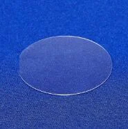
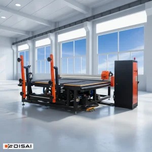
Cover glass for instrumentation and wear-resistant sapphire viewports are brittle and difficult to machine. Our advanced laser solutions use custom optical arrangements to create internal micro-cracks and clean separation paths, replacing traditional mechanical grinding processes.

Answering critical queries concerning industrial laser integration, wavelength selection, material compatibility, and customization parameters.
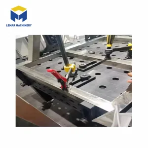
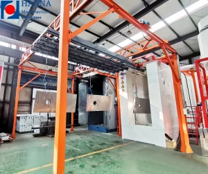
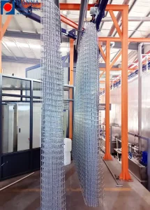
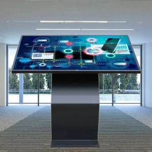
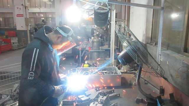
Explore additional specialized machinery including powder coating lines, heavy-duty welding platforms, and smart control interfaces developed for various industrial applications.
 Focus Laser